Starac
Chiplet-based Optical Network on Chip (ONoC)
Starac is a system-in-package demonstrator with a photonic interposer that enables all-to-all optical communications between chiplets. This approach to on-chip communications is ideal for increasingly complex systems-in-package with more and more chiplets or for chips made on increasingly large wafers.
The demonstrator features:
- Multiple compute chiplets
- I/O interface chiplets (drivers, data serialization, flow control, arbitration, routing, plus any application protocols)
- An optical network on chip (the photonic interposer)
- Rerouting BEOL for sideband signaling (synchronization)
What it can do
This innovation addresses a variety of system-level computing challenges. It is of interest to large tech firms or chip makers, startups, datacenters, and other organizations with high-performance or exascale compute projects.
- CEA-Leti can transfer a complete system or discrete technology bricks and manufacture test batches.
- Companies can co-develop hardware and architectures with CEA-Leti for a unique system tailored to their needs.
CEA-Leti brings its silicon photonic, very-large-scale integration, and architecture and circuit design expertise to R&D partnerships on this technology.
|
What makes it unique
With passive interposers, communication between chips is limited to “nextdoor neighbors.” With Starac’s photonic interposer, efficient communication between faraway chips becomes possible thanks to:
- A comprehensive state-of-the-art 3D silicon photonic platform
- A world-first optical network on chip topology
- Electro-optical drivers with 5X greater energy efficiency than CMOS routing
- A low-latency, non-blocking protocol for integration with compute that is 4X more efficient than synchronous CMOS transfers
- An optical routing architecture that would be impossible on a passive interposer
|
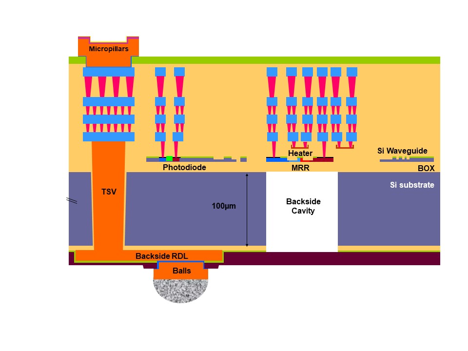
 Cross-section of silicon photonic interposer
What’s next
The current demonstrator is the result of four years of research at CEA-Leti and CEA-List. Further development work will focus on scaling up the 3D and photonic technology platforms to 300 mm as part of the EU Prevail project.
Publications
Main publications:
- Y. Thonnart et al., “POPSTAR: a Robust Modular Optical NoC Architecture for Chiplet-based 3D Integrated Systems,” Proc. DATE, 2020, p. 6
- D. Saint Patrice et al, “Process Integration of Photonic Interposer for Chiplet-Based 3D Systems,” ECTC 2023
|