CEA-Leti recognized for its expertise on bonding
The first collaboration between ASML and CEA-Leti began in 2018 as part of a study on the fabrication of 28nm and sub 28nm FD-SOI (Fully Depleted Silicon On Insulator) technologies. In more specific terms, the goal was to investigate the influence of SOI substrates on local constraints, which impact the critical issue of alignment between different levels of lithography. The success of the first study led to a second phase being launched in order to understand the challenges of integrating these new technological findings with sub-10nm nodes through the use of advanced bonding techniques, a field in which CEA-Leti has earned international recognition.
With the improved performance of wafer-to-wafer bonding and layer transfer techniques, new innovative architectures were introduced to simplify integrated circuit manufacturing technologies. This enabled an increase in the number of transistors per mm². For example, one of these new techniques involves stacking two layers of transistors, thus doubling their density for an equivalent surface area. In order to meet quality requirements, these stacked layers must not only be precisely positioned, but also extremely flat, so as not to lessen the nanometrically precise alignment that is required.
Through their collaboration, ASML and CEA-Leti are committed to developing technological solutions that will enable manufacturers to implement these new processes and thus meet the industrial challenges of manufacturing advanced circuits for 2026 and beyond.
“CEA-Leti and ASML skillsets are truly complementary,” notes Michael May, lithography engineer at CEA-Leti. “On our side, we can take advantage of equipment produced by ASML to carry out our research work. And ASML relies on our expertise to assess the impact of direct bonding on its component manufacturing processes.”
For instance, this technique results in a deformation of the wafers, which influences the effects of lithography. It is essential for this factor to be accounted for as early as possible.
A first-of-its-kind immersion scanner for a European research center
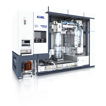
The ASML/CEA-Leti joint laboratory reached a new milestone with the installation of a TWINSCAN NXT:2050i immersion scanner produced by the company.
“Compared with so-called 'dry' lithographic scanners, immersion systems replace the air that is located between the projection lens and the plate with water,” explains Michael May. “It’s a unique feature that will enable us to achieve smaller etching sizes.”
This technology is not in and of itself new as the equipment acquired in 2018 as part of the joint laboratory already included an immersion scanner. However, the NXT:2050i model offers improved alignment precision between two successive layers (at the nanometric level). It is a first for a device of this type to be installed in a European research center.
“Thanks to this new immersion scanner, we will be able to meet the development requirements of 10 nm and 7 nm FD-SOI technologies, which is a subject CEA-Leti is fully committed to as part of the France 2030 investment program and the FAMES pilot line in the frame of the European Chips Act,” announces Nacima Allouti, head of industrial partnerships for the Silicon platform at CEA-Leti. “This collaboration is beneficial for both organizations as it enables CEA-Leti to remain at the forefront of technological research development while providing ASML with the ability to optimize the performance of its equipment in order to remain the world leader of lithography and metrology equipment.”
To achieve these objectives, the two organizations decided to renew their partnership with the aim of fostering European synergies in the field of semiconductors thanks to the participation of ASML, CEA-Leti and other major European players.

TWINSCAN NXT:2050i - Credits: ASML
Acknowledgments:
The first ASML equipment was partially funded by the Auvergne Rhône Alpes region and R&D was supported by the Auvergne Rhône Alpes region and the French State through the Nano2022 Program.
The NXT 2050i purchase was funded by the grant “ANR622-NEXG-0001” (NextGen project) from the French State related to France 2030 program managed by the National Research Agency
The NextGen project is also the national funding part of the FAMES Pilot Line of the Chips JU, also partly funded by Horizon Europe and Digital Europe Programmes.