Quantum packaging
A multi-chip assembly with quantum processor and control chips
This CEA-Leti demonstrator shows how the control electronics necessary for quantum processors can be migrated into the cryostat to support the scalability of quantum bits.
A silicon-based interposer connects the control and readout circuits with the qubit chip. Connections between the chips and the interposer are made using flip-chip techniques. Routing is ensured by superconducting interconnections, which provide solutions for thermal management, especially to protect the qubits from the heat generated by the control electronics. Finally, a cryopackage with a copper socket further improves overall system thermalization and protects the demonstrator from electrostatic disturbances.
What it can do
This demonstrator offers an integration platform compatible with any type of qubit made using any material or technology. CEA-Leti can also offer specific interposer designs to meet different qubit and system requirements. Plus, the interposer can comprise several superconducting routing layers offering various design and thermal management solutions. Beyond quantum computing, these technologies can be used for any superconducting applications and for certain space applications. The demonstrator leverages research conducted under the CEA’s quantum program, the ERC Synergy Grant 'QuCube' and the French National initiative 'France 2030' through the PEPR 'PRESQUILE' and CEA-Leti's joint lab with Quobly.
|
What makes it unique
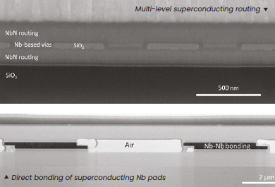
Multi-level routing enables denser interconnections between the chips in the assembly, as well as design solutions for carrying radiofrequency signals. Passive components for signal filtering, qubit control, and readout can also be integrated in this routing architecture. Direct bonding of superconducting niobium (Nb) pads at a pitch of 7 μm is also possible, providing an alternative with better superconducting properties than indium bumps for die-bonding, and opening the door to much smaller pitches.
|

What’s next
Upcoming developments include:
- Increased interconnection density and number of routing levels
- Superconducting TSVs & UBMs
- Study of thermal properties at interconnection and system levels
- Multi-partner large-scale quantum initiative (IRT LSQ) expected to start soon
Publications
- C. Thomas et al., Superconducting routing platform for large-scale integration of quantum
technologies, Materials for Quantum Technology, 2, 035001, (2022).
- C. Thomas et al, Die-to-Wafer 3D Interconnections Operating at Sub-Kelvin Temperatures
for Quantum Computation, ESTC 2020 (best paper).
- C. Thomas et al., Integration of planarized Nb-based vias to form a multi-level superconducting
back-end-of-line, ECTC 2024.
- P. Renaud et al., Fine pitch Nb-Nb direct bonding for quantum applications, ECTC 2024.
|