Structural anomalies in 2D materials have been known as the key to locally modifying their electrical, optical, and magnetic properties. In order to tailor the material properties and to explore their functionalities, the ability to survey the local electric properties together with their structural configuration at the atomic scale is essential. Recently a new imaging technique, sensitive to local electrostatic fields, has been demonstrated in so-called 4-Dimensional Scanning Transmission Electron Microscopy (4D-STEM) imaging mode. However this technique is not yet routinely used for the study of 2D materials due to the lack of quantitative understanding and interpretation of the reconstructed images.
The IRIG team used 4D-STEM to investigate a vanadium-doped WSe2 monolayer grown by molecular beam epitaxy. The reconstructed atomic-scale images of the electric field and electrostatic potential were compared with
ab initio-based STEM image simulations, accounting for important microscope parameters such as probe aberrations. This has finally led to a quantitative agreement between the experimental and simulated electrostatic potential reconstructions. Interestingly, a significant potential drop around the majority of vanadium dopant atoms was detected and attributed to the presence of negative charge (Figure) clearly demonstrating the capacity of 4D-STEM to reveal important information going beyond mere structural analysis.
Finally the technique was used to image the electrostatic potential landscape in more complex structural configurations, particularly in the presence of growth-related defects such as Se vacancies and inversion domain boundaries, opening the perspective for atomic-scale analysis of charge effects and interactions between charged defects in synthesized 2D materials.
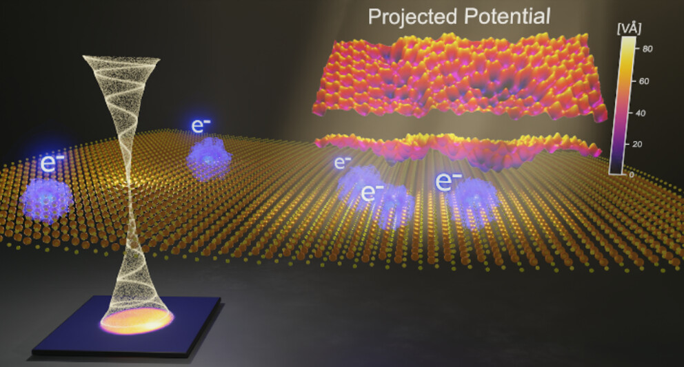
Figure: Illustration of potential mapping using 4D-STEM, highlighting the presence of negative charges inducing electrostatic potential drops around dopant atoms. Credit ACS Nano
4D-STEM offers a powerful approach for probing local electrostatic fields and potential landscapes at the atomic scale. The demonstrated capacity to quantitatively analyze charge states of individual dopants and defects complexes, such as those found in vanadium-doped WSe2, highlights the potential of this technique for advancing the understanding of 2D materials and their functional properties.
Collaboration
IRIG/Spintec for MBE growth
IRIG/MEM and UC Louvain (Belgium) for ab initio simulations
Institut Néel for 4D-STEM data processing