Intense compact THz sources in the microwave to far infrared range are the focus of major research and development. This low-energy, non-ionising radiation has numerous applications in medical imaging, molecule identification and security.
In 2016, a new principle for generating THz waves emerged, based on the ultra-fast conversion of a spin current into a charge current. The resulting THz transmitter, known as "spintronics", is as intense as competing technologies, but has the advantage of being broadband. In scientific terms, it is also a formidable tool for characterizing and quantifying spin-to-charge conversion mechanisms in materials. Researchers at IRIG have analyzed THz emission according to the nature, symmetry and number of layers in 2D materials.
The structure of 2D materials gives them a number of advantages, including the ability to manufacture ultra-compact devices that are simpler to use than 3D materials (in particular, their ultimate thickness means that they can be shaped very quickly by etching), and requiring less material for more sustainable electronics. Moreover, their high sensitivity to the chemical or electrical environment makes it easy to modulate their electronic properties, such as spin-orbit coupling, the key ingredient of spin-charge interconversion. The fabrication of heterostructures with perfect interfaces by stacking 2D layers with van der Waals type bonds offers an infinite number of combinations of materials to optimize these effects, particularly for THz emission. More generally, the fundamental study of the conversion between spin currents and charge currents in 2D materials is essential before considering their integration into spintronic devices, such as magnetic memories or sensors.
However, there are two obstacles to the development of such THz sources: the manufacture of 2D materials over large surfaces, and the control of the interface between a 2D material and a ferromagnetic electrode. Laboratory 2D materials are generally small in size because in the form of micrometric flakes mechanically exfoliated from a bulk material. In addition, the interface between the 2D material and the ferromagnetic material that is the source of spin current is never well defined: the growth of this electrode on the 2D material leads to interface chemical reactions and atomic interdiffusion. The researchers succeeded in overcoming these two obstacles to study the spin-charge conversion mechanisms in PtSe2 platinum diselenide.
For the past 10 years, the IRIG team has been developing ultra-high vacuum molecular beam epitaxy (MBE) growth of 2D single crystals of transition metal dichalcogenides (TMD) over large surfaces of several cm2. The ferromagnetic material was then deposited in the same ultra-high vacuum chamber under growth conditions optimized to obtain perfect interfaces (see inset in
Fig. 1).
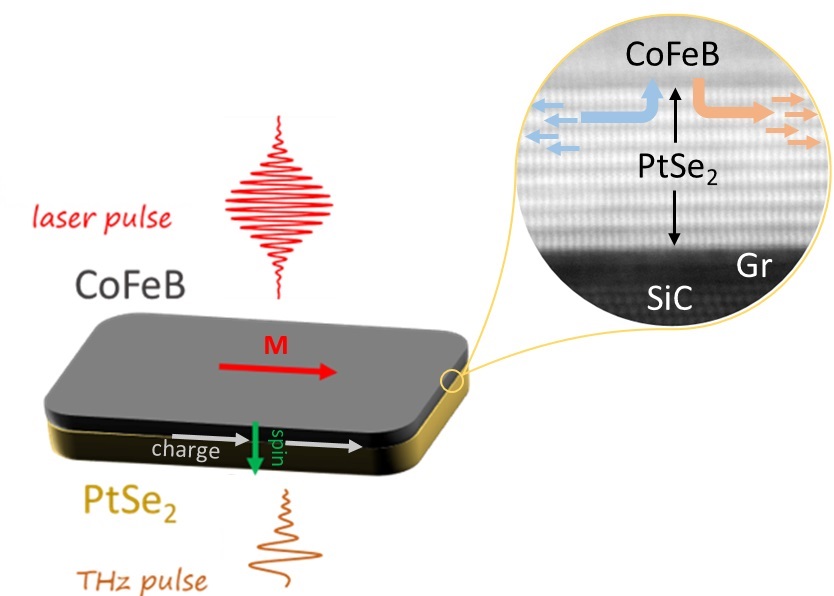
Figure 1: schematic diagram of THz emission from a CoFeB/PtSe2 bilayer excited by a femtosecond laser pulse. Inset: an atomic-scale zoom of the electron microscopy image of the stack of 8 PtSe2 monolayers epitaxially grown on graphene/SiC, showing the quality of the interfaces. The opposite movement of the 'up' (blue) and 'down' (brown) spins perpendicular to the layers is called the spin current. It is associated with the longitudinal charge current in the plane of the layers. Credit CEA
To identify and quantify the conversion mechanisms, the spintronic characterization technique using THz frequency emission is easy to implement and does not require any other technological process. It is also highly sensitive and non-destructive (Fig. 1).
The PtSe2 material exhibits an intense THz signal, making it possible to study the emission as a function of the number of monolayers (ML). Remarkably, the curve in Fig. 2 shows a step at 4 ML, which corresponds exactly to the electronic transition from the semiconductor to the semi-metallic state of the material. At low thicknesses (< 4 ML) in the semiconducting regime, the charge transfer between the graphene substrate and the first layer of PtSe2 creates an interface electric field, and also a Rashba-type spintronic effect at the origin of the spin-charge conversion and the THz signal (Fig. 2). In this regime, it would be possible to modulate the THz emission by applying an external electric field. For thicker layers (> 4 ML), the transition to the semi-metallic state adds the phenomenon of conversion called the spin Hall effect, which corresponds to a volume effect (Fig. 2). Theoretical studies have validated this interpretation and quantified these effects, combining a simple spin diffusion model and
ab initio calculations.
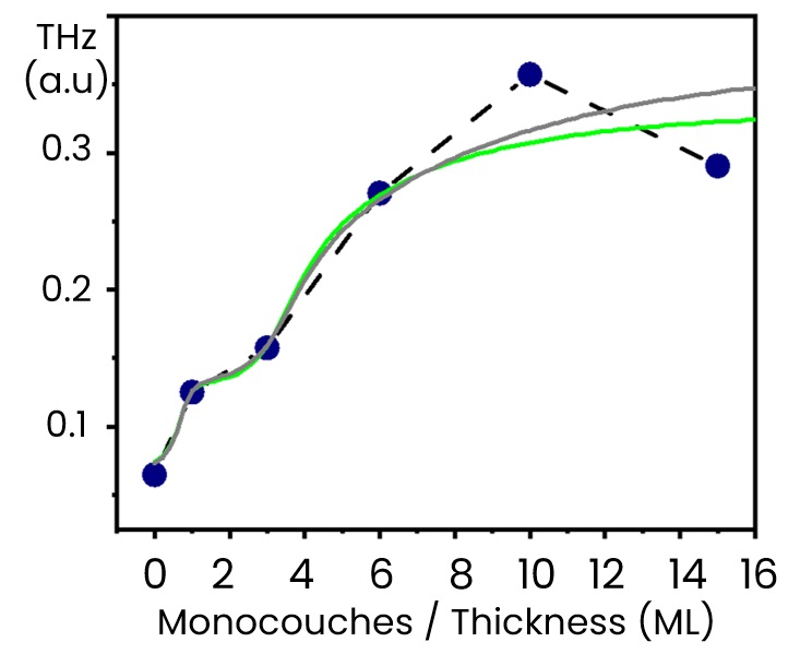
Figure 2: measurements of the intensity of the THz electric field emitted as a function of the thickness (in number of monolayers or ML) of PtSe2 showing two conversion regimes at low thicknesses (< 4ML) and high thicknesses (> 4ML). The blue dots correspond to measurements and the solid lines to theoretical fits. Credit CEA
In conclusion, 2D materials open up new horizons for spintronics and the emission of THz waves sustainably and in a tunable way.
Collaboration
- Irig/MEM, Irig/SyMMES et Irig/Pheliqs
- Laboratoire de Physique de l'Ecole Normale Supérieure LPENS, Paris
- Laboratoire Albert Fert LAF, Palaiseau
- Centre de Nanosciences et Nanotechnologies C2N, Palaiseau
- Institut Néel, Grenoble